ID10 NanoProbe
1. Introduction
2. Scientific objectives
The nanoprobe beamline provides a nano-beam smaller than 50 nm in the hard X-ray energy range of 5 to 25 keV. This beam size of 50 nm allows for quantitative nanoscale analysis of the element distribution and quantity of materials in localized regions. The energy range of 5 to 25 keV enables quantitative nano-spectroscopy for most transition metals and rare earth metals. Additionally, the high penetration power of hard X-rays can pass through gas environments and windows for maintaining environments. This allows for the study of materials under synthesis and operating conditions. To facilitate such research, the nanoprobe beamline is designed to provide a long working distance of 50 mm despite the small beam size in the tens of nanometer range. This makes it easy to insert devices that offer various conditions, such as high and low temperature, gas environments, liquid environment sample delivery, and the application of electric or magnetic fields, enabling in-situ/operando materials research. The scientific objectives of the nanoprobe are on tracking the reactions and defect growth processes of battery and catalyst systems, and the quantitative nanoscale analysis of complex functional materials and material systems in actual manufacturing and operating environments. Also, to accommodate with the trend of scaling up systems by spreading and stacking nano-components for enhanced reactivity and performance, we have introduced high-speed precision nano-stages, allowing us to investigate larger areas at the nanoscale. The signal recording equipment includes X-ray fluorescence detectors and signal detectors, providing quantitative simultaneous information on the electron density, strain, and element distribution of the sample, with all experiments designed to be studied in three dimensions.
3. Beamline Requirements for the Insertion Device
The nanoprobe beamline provides an energy range of 5-25 keV using an In-Vacuum Undulator(IVU). IDs of Nanoprobe are designed to give the highest brilliance in this range without losing energy continuity. The parameters for the IDs are detailed in Table 1. The maximum power represents the maximum beam power passing through a mask with a 2 x 2 mm² opening @ 23 m under the maximum current conditions(400 mA) [Table 1].
Undu lator |
Period [mm]* |
Length [m]* |
Location |
Max P ower |
Min. Gap [mm] |
|---|---|---|---|---|---|
In -vacuum |
24 |
3.0 |
Center of Straight section |
0.96 kW |
6 |
Table 1. Parameters of insertion device
4. Beamline Requirements for the Front End
The FE of the nanoprobe beamline is required to 1) handle a 17 kW heat load, 2) beam position diagnostics, and 3) radiation safety. First, the 17 kW total beam power generated by the IDs is managed using three masks with water cooled channels. Two of these masks are ‘Movable masks’ with adjustable gap sizes and positions, while the third is a ‘Fixed mask’ with a fixed aperture size in horizontal direction that can only have its position adjusted. For detailed specifications of the masks, refer to Chapter []. Note that although the IDs have a minimum gap of 5 mm, the effective minimum gap required to provide the 5-25 keV range is 6 mm. Consequently, the effective maximum total power of nanoprobe IDs is 12 kW. Secondly, the FE includes an X-ray beam position diagnostic device. In the first phase, the diagnostic X-ray beam position will be used to provide feedback for slits position, ensuring the stability of the beam intensity delivered to the sample within 10%. In the mature phase, the diagnostic X-ray beam position will also be integrated with the electron beam feedback system to enhance performance. For detailed specifications of the diagnostic device, refer to Chapter []. Lastly, the FE is equipped with safety devices to protect against gamma radiation and electron beam insertion in FE. Especifically, a safety magnet with a strength of 0.5 T is installed to handle scenarios where the electron beam enters the FE. This ensures that any electron beam inserted into the FE is deflected horizontally and prevented from reaching the optical hutch.
5. Beamline Layout
Beamline layout
The Nanoprobe beamline is one of the two “long beamlines” being developed for the Korea-4GSR construction.
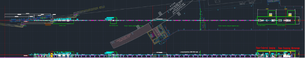
[Figure 1] Beamline layout of Nanoprobe beamline
Beamline component list
Distance (m) |
Component name |
D es cr ip ti on / C om me nt |
|
|---|---|---|---|
0 |
IVU24 |
||
27.0 |
Beam attenuator |
D ia mo nd 0 .5 mm - 3 mm th ic k, S il ic on 0 .5 mm - 10 mm t hi ck |
|
28.0 |
White beam slit |
Up to 4 kW he at lo ad |
|
28.8 |
Diamond screening monitor |
Re so lu ti on 1 um D ia mo nd t hi ck ne ss 2 00 um Be am mo ni to ri ng |
|
29.0 |
Horizontal high heat load mirror (Sagittal focusing) |
S ph er ic al cy li nd er mi rr or 3 -s tr ip c oa ti ng (P t, R h, S i) |
|
29.8 |
Diamond screening monitor |
Re so lu ti on < 1 um /D ia mo nd t hi ck ne ss 2 00 um |
|
30.4 |
Horizontal mirror (Tangential focusing) |
El li pt ic al cy li nd er Be nd ab le mi rr or 3 -s tr ip c oa ti ng (P t, R h, S i) |
|
31.0 |
White beam diamond beam position monitor |
Re so lu ti on be am si ze < 0. 1% / Be am po si ti on m on it or a nd be am po si ti on fe ed ba ck wi th mi rr or sy st em |
|
32.0 |
DCM |
HD CM Of fs et < 10 mm |
|
35.0 |
Diamond beam position monitor |
Re so lu ti on be am si ze < 0. 1% / Be am po si ti on m on it or a nd be am po si ti on fe ed ba ck wi th mi rr or sy st em |
|
57.0 |
Nanobeam position monitor and screening |
Re so lu ti on 1 00 nm ta rg et a ng le re so lu ti on < 50 nr ad |
|
58.0 |
Secondary source aperture (Precision slit) |
G ap re so lu ti on ~ 1 00 nm / M in im um g ap 1 um |
|
137.0 |
Beam position monitor |
D ia mo nd sc re en mo ni to r, 1 um r es ol ut io n, R em ov ab le |
|
138.0 |
Endstation 1 |
||
147.0 |
Beam position monitor |
D ia mo nd sc re en mo ni to r, 1 um r es ol ut io n, R em ov ab le |
|
148.0 |
Ion gas chamber |
||
149.0 |
KB mirror slit |
4 -w ay Sl it s, HV / Re mo ve p ar as it ic sc at te ri ng |
|
149.5 |
KB mirror and chamber |
H: 3 00 m m, V: 1 00 m m, P t, R h, Si c oa ti ng In ci de nt an gl e: 3 mr ad |
|
150.0 |
Endstation 2 |
[Table 2] Major component list of Nanoprobe beamline
6. Optics Overview
In this section, we describe the optics and beam specifications of the nanoprobe beamline. For parameters related to the electron beam, refer to the chapter []. All optical simulations were performed in ShadowOui with the OASYS environment. The simulations for the optical components were primarily conducted at 10 keV, which is expected to be frequently used, and also at 20 keV for comparison. Note that the X-ray beam source parameters provided by the OASYS environment do not take into account the electron energy dispersion. This means that the divergence angle of the beam is smaller than twice at high energies (high harmonics). Thus, we use the source parameters provided by SPECTRA as a Geometry source in OASYS. Also, the coherent length (BDA gap size) and coherent flux calculations were conducted using homemade code in the Matlab environment.
Beam specification
Energy |
BDA-V |
BDA-H |
|---|---|---|
10 keV |
2.6 µm |
2.5 µm |
20 keV |
1.6 µm |
1.5 µm |
[Table 3] The coherence length at the BDA.
[Table 3] shows the coherence length at 10 keV and 20 keV. This represents the coherence size of the beam focused at the BDA position, which is a crucial factor for coherence diffraction(scattering) experiments (e.g., Ptychography, XPCS). [Table 4] shows the coherence fraction, which is the ratio of the total flux to the coherent flux in a mono beam. Coherent flux is the flux passing through the BDA when it is opened to the coherence length. [Figure 2] shows the expected coherent flux delivered to the sample, taking into account mirror reflectivity, number of reflections, BDA size, angular acceptance of the nanofocusing optics, and the polarization effect of the HDCM.
E nergy |
Coherent flux (phs/s) |
Total flux (phs/s) |
Coherent fraction |
|---|---|---|---|
10 keV |
4.85 x 10¹² |
7.42 x 10¹³ |
6.5 % |
20 keV |
4.03 x 10¹¹ |
2.85 x 10¹³ |
1.4 % |
[Table 4] Flux and coherent fraction.
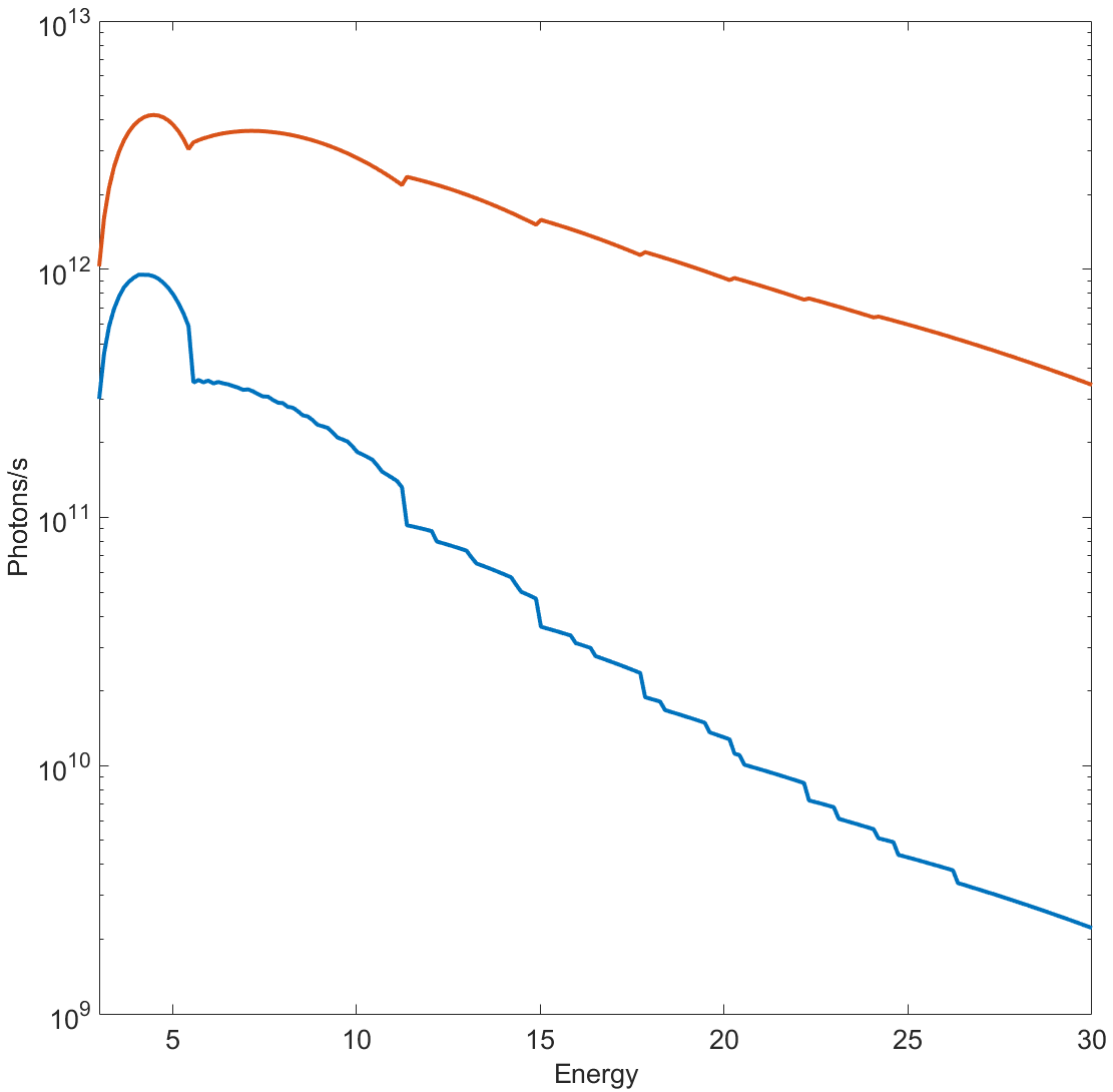
[Figure 2] Total photon flux(red) and photon flux of single coherence mode(blue) @ sample position
Consideration for optical layout

[Figure 3] Optical layout of Nanoprobe beamline. M1(High heat load mirror, Sagittal focusing) and M2(High heat load mirror, Bendable, meridional focusing) are horizontally reflecting mirrors. HDCM is Horizontal deflecting Double Crystal Monochromator. SSA is a secondary source aperture, also called a Beam defining aperture (BDA).
[Figure 3] shows the optical layout of the nanoprobe beamline. The ultimate goal in designing the layout and specifications of the optical components is to keep the beam instability delivered to the sample below 10%. To achieve this, we are considering two main aspects. First, the beamline layout of the nanoprobe beamline incorporates a secondary source focusing method that enables a flux-versus-resolution trade-off using the BDA. The optimal position for the BDA is determined by the coherence length at the BDA position. An optical design with a high magnification ratio at the BDA allows for a shorter beamline with lower construction costs. However, the engineering challenge lies in making controllable apertures smaller than a micrometer. [Table 5] shows the coherence length and RMS beam size at the BDA for different magnification ratios. A magnification ratio of approximately 1:1 provides a controllable aperture size. The first optics after the shielding wall is 29 m from the source, and thus BDA optimal position is 58 m.
E nergy |
Magnification |
2:1 |
1:1 |
1:2 |
|---|---|---|---|---|
10 keV |
Coherence length (H x V, um) |
1.28 x 1.34 |
2.5 x 2.6 |
3.9 x 4.0 |
RMS beam size (H x V, um) |
9.8 x 2.3 |
19.0 x 4.5 |
29.4 x 7.0 |
|
20 keV |
Coherence length (H x V, um) |
0.77 x 0.84 |
1.5 x 1.6 |
2.3 x 2.5 |
RMS beam size (H x V, um) |
9.8 x 2.2 |
18.9 x 4.2 |
29.3 x 6.5 |
[Table 5] The coherence length and RMS beam size at the BDA for different magnification ratios.
Second, the design ensures that the peak heat density on the DCM is kept below 40 W/mm². This is to prevent thermal bumps and damage of the first crystal. To reduce the heat density, beamlines of Korea-4GSR adopt two strategies. The first is to locate the DCM crystal more than 50 m away from the source. This approach minimizes the number of optical components. Also, this prevents wavefront distortion caused by imperfections of mirror surface and beam instability caused by optics vibrations. However, this strategy cannot optimize the beam flux. Because it can only accept a limited beam flux that does not cause thermal bumps. The second is using a High Heat Load Mirror(HHML). This has the drawback of needing to correct the thermal bump [Figure 4]. Thermal bump correction strategy using a benting pre-focusing mirror can provide high beam flux above 1012 phs/s (Coherence flux: >1011 phs/s @ 10 keV). One of the objectives of a nanoprobe beamline is to rapidly investigate a wide sample in nanoscale resolution, as mentioned in the scientific objective section. To achieve this, beam flux maximization is necessary. Thus, we have chosen the second strategy.
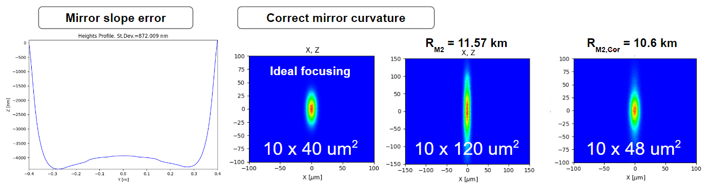
[Figure 4] Mirror surface profile caused by thermal bumps on the M1 mirror. The mirror slope error graph shows the thermal bump profile when the maximum total power is delivered to the HHLM with the notch design applied. Bend M2 to correct the focused beam size at the BDA to be closer to the ideal size.
Optics Specification
M1 |
M2 |
DCM |
|
|---|---|---|---|
Source to sample distance (m) |
29 |
30.4 |
32 |
Incident Angle |
2.5 mrad |
2.5 mrad |
3 ~ 45 degree |
Shape |
Fixed spherical cylinder |
Bendable spherical cylinder |
Plane |
Radius (mm) |
Rs : 72.5 / Rm : > 100 km |
11.6 km |
Inf |
Direction |
Horizontal |
Horizontal |
Horizontal |
Substrate |
Si |
Si |
Si |
Coating Material |
Pt (40 nm) |
Si, Pt (40 nm) |
|
Mirror size (H × V, mm × mm) |
400 x 30 |
400 x 30 |
|
Focal length (mm) |
29,000 |
27,600 |
Inf |
Roughness σ (nm) |
< 0.3 |
< 0.3 |
< 1 |
Slope error (μrad, RMS) |
< 0.2 |
< 0.2 |
< 1 |
Max. total heat load (W) |
36.4 |
20.6 |
102 |
Max. surface head load (W/mm2) |
0.093 |
0.016 |
< 40 |
[Table 6] M1, M2 mirrors specification
[Table 6] lists the specifications of the mirrors used in the nanoprobe beamline. The specifications of the M1 and M2 mirrors are designed to focus the beam on the BDA located at 58 m. The slope error tolerance is set to ensure that the beam broadens and intensity decreases below 10%. The M3 mirror is a Nano-KB mirror designed to produce a beam of <50 nm at energies above 8 keV. The M3 mirror also has less than 10% beam broadening and intensity decreases with its set slope error and roughness tolerance. [Figure 5] shows the results of a simulation of the beam delivered to the sample when these tolerances are met.
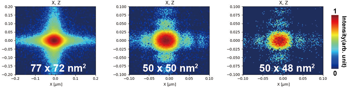
[Figure 5] Effects of KB mirror slope errors on the focused beam. (Left) SSA full open, (Middle) SSA 18.6 x 6.2 um2 open, (Right) SSA 5 x 5 um2 open. Colormap scale is logarithmic.